
via in pads
The use of via in pad has become increasingly popular in PCBs, especially those that require high-density interconnect (HDI). This technology helps designers minimize the size of their circuit boards while maintaining good signal integrity. However, it comes with certain risks and challenges that must be addressed to ensure its success. In this blog post, we’ll discuss three of the biggest myths surrounding via in pad and help you determine whether it’s the right solution for your next design.
The first and most common reason for a manufacturer to recommend the use of via in pad is to improve thermal management. This is especially important in small form factor devices, such as smartphones and wearables, where space is at a premium. Via in pads allow for a more direct path from the component to the ground plane, which allows it to dissipate heat more effectively.
Another common use of via in pad is to increase the signal integrity of a circuit board. By placing vias close to the signals they connect, via in pad can reduce the amount of current flowing through the connection point and prevent signal distortion.
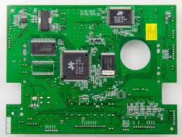
Are via in pads used in all types of PCBs?
Finally, via in pad is a great option for high-speed signals, as it can improve the velocity of the signal by reducing parasitic inductance. Since the via is directly connected to the pad, it has a much smaller resistance and capacitance than traditional through-hole vias.
As the number of components in a PCB increases, placement and routing issues can become challenging. To make up for these difficulties, many designers choose to place a via in the pad to save space on surface layers. However, it is important to note that via-in-pad placement is not suitable for all applications, and there are certain myths surrounding this practice that should be avoided at all costs.
In order to avoid problems during assembly, the via holes must be filled and capped before the components are placed on the board. This process involves coating the hole with a conductive or non-conductive epoxy, then plating over it with copper. Regardless of the type of via, this cap is necessary to prevent solder wicking during the reflow process and ensure that the pads on which the via is located have enough copper to make a reliable connection with the component.
Another problem that can occur with via in pads is that the plated over area of the pad may be too thick to accept a standard IPC class 1 breakout. This issue can be overcome by using a special technique called via tenting, which involves coating the surface of the drilled hole with a layer of solder mask that resists the flow of solder.
Despite the advantages of via in pad, it is important to remember that this technique requires more attention during the fabrication and assembly processes, which can increase PCB Turnaround Time. For this reason, it is crucial that you choose a fabrication partner who has the experience and equipment needed to implement this technology effectively. With the right manufacturing partner and proper PCB layout, via in pad can be a valuable tool for improving the performance of your circuit board.
