
PCB Fabrication Assembly
PCB fabrication assembly is the process of taking a schematic or idea from its design phase to a fully functional prototype. In order for this to happen, the PCB must undergo several stages of development, manufacturing and testing. During this time, the board’s layout must be approved by engineers and the correct materials selected. Once the board passes through all of these checks, it can be sent to the fabrication plant for final assembly.
The pcb fabrication assembly process starts with a laminate panel, or the base of the circuit board. The panel is then covered with a photo-sensitive film called resist, which contains a layer of photo-reactive chemicals that polymerize when exposed to ultraviolet light. A computer-controlled laser then scans the panel and creates a digital image. This image matches up with a pre-loaded CAD/CAM design file. This digital image is then printed to the panel through a special printer known as an LDI, or laser direct imaging. The registration holes in the laminate act as guides to align these images as they’re printed.
Once the images are printed, copper is deposited onto both sides of the panel using an electroless or chemical deposition method. This is followed by etching, which removes the areas of copper that won’t be in the final product. After the etching process, an automatic optical inspection machine (AOI) scans the panels to confirm that there are no errors in the digital image. If the AOI scan detects an error, it is flagged and passed over for manual review.
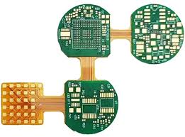
How is PCB Fabrication Assembly Made?
At this stage, the contract manufacturer (CM) will order the appropriate components for the circuit board’s design. This includes all of the necessary parts to assemble the through-hole components on the board and the solder paste needed to connect these parts. The CM will also place an order for the substrate material. Different types of substrate material are available, but the most common is a glass-fiber reinforced epoxy laminate, or FR-4. Other options include phenolics, ceramics and metal core materials.
When the components are delivered, they are inspected for compatibility with the original design and for defects like missing parts or incorrect connections. Once the components have been inspected, the PCB goes through a series of electrical tests. These tests look for characteristics such as signal output, voltage and current fluctuation and peaks that don’t fall within the expected range. If the PCB fails these tests, it must go back to the CM for repair and retest.
Once the PCB has passed all of the electrical tests, it’s ready for assembly. The CM will score the boards with a V cut on their outline, or route out most of the board except for small breakout tabs. The resulting PCBs must pass a physical test, which looks for sharp edges or burrs that could cause problems with the final product’s functionality. Then, the CM will either assemble the circuit board themselves or send it to another company for component assembly.
