
Minimize Defects in PCB Manufacturing Assemblies
The PCB manufacturing process is prone to multiple defects, and it’s important to understand the issues to address them. Comprehensive training programs, detailed work instructions, job aids like checklists, increased automation and redundancy through items like secondary verification of machine setups all help reduce human error. Additionally, careful material selection, meticulous manufacturing processes, and quality inspection techniques help minimize defects.
Soldering is a particularly critical process for the assembly of a PCB. It is prone to numerous problems including bridges, voids, cold joints, tombstoning, and insufficient wetting. Maintaining a stable temperature, proper stencil design and precise application of solder paste are all key factors in avoiding these defects. Using a high-precision automatic optical inspection (AOI) system also helps detect and avoid these defects.
Acid traps – These occur when etching acids accumulate on the surface of a PCB and interfere with circuit functionality. PCB layout standards and careful use of chemical solutions can help reduce acid traps.
Defects specific to SMT – Surface mount technology (SMT) is a unique pcb manufacturing assembly method that requires specialized equipment, training and expertise. SMT components are mounted with a special soldering system that uses tin-copper solder. SMT components are typically smaller than traditional components, which increases the risk of errors in handling and mounting. Maintaining strict SMT production protocols and quality control, utilizing advanced SMT inspection systems, and implementing Design for Manufacturability guidelines (DFM) can help reduce these unique PCB assembly problems.
Dimensional defects – These include Skew (shifting of inner layers), Pattern misregistration, incorrect hole alignment, out-of-tolerance features, annular rings (circular areas around drilled holes), and board warpage (abnormal flatness). Maintaining tight tolerances on all PCB dimensions is essential for assembly and performance. Correcting dimensional problems early in the fabrication process can help prevent costly delays in assembly.
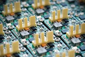
How to Minimize Defects in PCB Manufacturing Assemblies
Other common defects include open solder joints (no bonding at the component lead and pad), excessive solder bridging (connecting tracks that shouldn’t be connected), and missing or damaged traces. Proper spacing and clearances between components ensures efficient signal flow, reduces the risk of short circuits, and allows for easier troubleshooting.
Mechanical damage – Typical mechanical defects include dents, scratches, cracking, chipping and holes. Careful handling, protective storage racks, and consistent cleaning of etched and bare boards minimize mechanical defects. Contamination – Flux residues, finger oils, metal particles, chemical solutions such as etchants and plating baths, dust and debris can all contaminate a PCB. Staff training on contamination controls and keeping production areas clean reduces these risks.
DFM is a proactive approach that incorporates manufacturing considerations into the design phase. By following DFM guidelines, designers can identify and eliminate potential issues that could arise during manufacturing. This includes ensuring proper spacing between components, adequate pad sizes, and avoiding complex geometries that could lead to difficulties in assembly and increased defect rates.
Choosing high-quality raw materials for both the PCB itself and the components can significantly reduce defects. This includes using reputable suppliers for laminates, solder masks, and components, as well as ensuring that all materials meet the required specifications and standards.
Maintaining clear communication and collaboration between design, manufacturing, and quality assurance teams can prevent misunderstandings and errors. Regular meetings and reviews of design files, manufacturing plans, and test results can ensure that everyone is aligned and potential issues are addressed promptly.
