
common defects in flexible PCB fabrication
A flexible printed circuit board (PCB) can be subject to a variety of defects that can negatively affect its function. These defects can be due to design errors, manufacturing errors or handling issues. These defects can cause the circuit to malfunction or even fail. In this article, we’ll take a look at some of the most common flaws that occur in flexible PCB fabrication.
One of the most common flexible pcb fabrication flaws is cold solder joints. This occurs when the solder isn’t properly warmed up, which can result in a poor connection between components. Cold solder joints can also cause corrosion and oxidation, which can lead to poor electrical performance. This defect can be prevented by making sure that the solder is sufficiently warmed before it’s used.
Another common fabrication error is misaligned components. This can be caused by improper alignment of the components with their pads or a crooked orientation of the component on the PCB. This defect can be corrected by double-checking the component data sheet and blueprint to ensure that the components are positioned correctly.
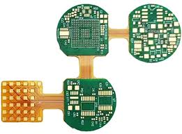
What are common defects in flexible PCB fabrication?
The etching process used in PCB fabrication can cause copper corrosion, which is characterized by an iridescent appearance on the surface of the circuit board. This corrosion can result in short circuits or open circuits, which can be fatal to the operation of the circuit board. To prevent this, the etching process should be carefully controlled to ensure that the copper coating is evenly distributed throughout the circuit board.
Other types of fabrication defects include voids in the plating process, lifted pads and traces, solder bridges, acid pits and other issues related to the handling of the PCB during assembly and shipping. To prevent these defects, manufacturers should use a high-quality PCB manufacturer and follow their recommended machining techniques.
Plating voids are gaps or holes in the plating, which can be the result of problems with the deposition process. These voids can allow unwanted connections to be made between pins, pads or circuit traces, which may result in short circuits or incomplete solder joints. The voids can be easily spotted by visual inspection.
Vias are at a higher risk of peeling from flex layers than from rigid ones, which can lead to failure in dynamic applications. This can be avoided by ensuring that the vias are as large as possible, by using annular rings and by adding tabs or anchors to the vias. In addition, vias should be placed over a stiffener rather than off of it, as this will reduce the stress concentration at the vias’ edges and improve their reliability in bending applications.
Another frequent problem is flex splitting, which occurs when the flex region is twisted or curved frequently. This can be prevented by determining the correct curve angle for the flex zone and by keeping the number of bends to a minimum. Additionally, the flex zone should be designed with enough space between the solder pads and their adjacent conductive traces to account for the difference in temperature expansion rates of rigid and flex circuit boards.
