

What are the main benefits of using HDI PCB?
High-Density Interconnect (HDI) PCB has become a cornerstone in modern electronic design, offering a range of advantages that make it an ideal choice for applications requiring high-performance and miniaturized components. HDI PCBs are distinguished by their advanced manufacturing techniques that enable more densely packed circuitry, allowing for smaller, more powerful, and reliable devices. Below are the key benefits of using HDI PCB in electronic manufacturing.
1. Increased Circuit Density
One of the primary advantages of hdi pcb is its ability to increase circuit density. Unlike traditional PCBs, HDI boards use finer traces and smaller vias, allowing for more components to be packed into a smaller space. This increased density is particularly beneficial for applications in compact electronics like smartphones, wearables, and medical devices, where space is limited but high functionality is essential. With HDI PCB, manufacturers can achieve a higher component density without compromising on performance or reliability.
2. Improved Signal Integrity and Performance
The high-density layout of HDI PCB helps in reducing signal loss and electromagnetic interference (EMI). By minimizing the distance between components and using blind and buried vias, HDI PCBs ensure that signals travel more directly through the circuit, reducing potential disruptions that can affect the performance of high-speed devices. This enhanced signal integrity is crucial for applications such as communication systems, automotive electronics, and high-frequency devices, where maintaining signal quality is paramount.
3. Smaller Form Factor
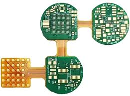
As electronic devices continue to shrink, so does the demand for smaller and more efficient PCBs. HDI PCB’s ability to integrate multiple layers and fine traces into a compact design makes it an ideal solution for manufacturers looking to reduce the size of their products without sacrificing performance. The small form factor offered by HDI PCBs is essential in industries like mobile devices, where portability and lightweight designs are critical to user experience.
4. Lower Power Consumption
Another significant benefit of using HDI PCB is the potential for lower power consumption. Due to the reduced trace lengths and smaller vias, the power required to transmit signals through the board is minimized. This not only helps in conserving battery life for portable devices but also reduces overall energy consumption, making HDI PCBs more eco-friendly. For portable electronics, such as laptops, tablets, and smartphones, this reduced power consumption translates into longer battery life, which is always a key selling point.
5. Better Thermal Management
The thermal performance of HDI PCBs is another standout feature. These boards are designed with materials that dissipate heat more efficiently, preventing overheating and ensuring stable performance even in high-power applications. Enhanced thermal management is critical in industries like automotive and aerospace, where high levels of heat can negatively impact both performance and safety. The superior heat dissipation of HDI PCBs ensures longevity and reliability in demanding environments.
6. Reduced Manufacturing Costs
Although the initial cost of HDI PCB production can be higher due to the advanced technology involved, the benefits they offer can lead to long-term cost savings. With smaller and more efficient designs, manufacturers can reduce the size of their overall product, potentially lowering material and shipping costs. Additionally, the enhanced reliability and durability of HDI PCBs can result in fewer failures and reduced warranty claims, leading to lower maintenance costs over the lifespan of the product.
Conclusion
HDI PCB offers a variety of benefits that make it the go-to solution for modern electronic designs. From higher circuit density and better signal integrity to smaller form factors and reduced power consumption, HDI PCBs are revolutionizing industries ranging from consumer electronics to automotive. As technology continues to advance, the use of HDI PCBs will only grow, paving the way for more powerful, efficient, and compact devices. By integrating HDI PCBs into their designs, manufacturers can meet the increasing demands for performance, miniaturization, and sustainability in today’s competitive market.

